Showing posts with label power. Show all posts

Saturday, January 11, 2014

Simple Power Switching Circuit Diagram

This Simple Power Switching Circuit Diagram provides on/off switching, soft starting, current monitoring, current tripping, and protection against over-current for a 30 Vdc power supply at normal load currents up to 2 A. The switch is turned on by an `on` command pulse; it is turned off by an `off` command pulse. An over-current trip can also be set on the bus side by a 6-digit binary signal, which is converted to an analog voltage and compared with the amplified voltage developed across a load-current-sensing resistor. 

Resistor/capacitor combinations (0.027 µ, 2 kfi) at the inputs of the current-sensing amplifiers act as low-pass filters: this introduces a few hundred /is of delay in the response to over-current, thereby providing some immunity to noise. The 0.022 µ capacitors connected to the drain terminals of the PFETs provide a Miller effect, which reduces the rate of change of the drain voltage and therefore the rate of rise of current at turn-on. The soft-turn-on time depends upon the load impedance and is typically 100 to 200 ms.

 Power Switching Circuit Diagram

Simple Power Switching Circuit Diagram

See More Detail[...]

Thursday, December 26, 2013

USB Powered Audio Power Amplifier

This circuit of multimedia speakers for PCs has single-chip-based design, low-voltage power supply, compatibility with USB power, easy heat-sinking, low cost, high flexibility and wide temperature tolerance. At the heart of the circuit is IC TDA2822M. This IC is, in fact, mono-lithic type in 8-lead mini DIP package. It is intended for use as a dual audio power amplifier in battery-powered sound players. Specifications of TDA2822M are low quiescent current, low crossover distortion, supply voltage down to 1.8 volts and minimum output power of around 450 mW/channel with 4-ohm loudspeaker at 5V DC supply input.

An ideal power amplifier can be simply defined as a circuit that can deliver audio power into external loads without generating significant signal distortion and without consuming excessive quiescent current. This circuit is powered by 5V DC supply available from the USB port of the PC. When power switch S1 is flipped to ‘on’ position, 5V power supply is extended to the circuit and power-indicator red LED1 lights up instantly. Resistor R1 is a current surge limiter and capacitors C1 and C4 act as buffers. Working of the circuit is simple. Audio signals from the PC audio socket/headphone socket are fed to the amplifier circuit through components R2 and C2 (left channel), and R3 and C3 (right channel)

USB Powered Audio Power Amplifier Circuit diagram:

USB Powered Audio Power Amplifier Circuit Diagram

Potmeter VR1 works as the volume controller for left (L) channel and potmeter VR2 works for right (R) channel. Pin 7 of TDA2822M receives the left-channel sound signals and pin 6 receives the right-channel signals through VR1 and VR2, respectively. Ampl i f ied signals for driving the left and right loudspeakers are available at pins 1 and 3 of IC1, respectively. Components R5 and C8, and R6 and C10 form the traditional zobel network. Assemble the circuit on a medium-size, general-purpose PCB and enclose in a suitable cabinet. It is advisable to use a socket for IC TDA2822M. The external connections should be made using suitably screened wires for better result.
Sucre:  http://www.ecircuitslab.com/2011/06/usb-powered-audio-power-amplifier.html
See More Detail[...]

Friday, December 20, 2013

Linear RF Power Meter

The National Semiconductor LMV225 is a linear RF power meter IC in an SMD package. It can be used over the frequency range of 450 MHz to 2000 MHz and requires only four external components. The input coupling capacitor isolates the DC voltage of the IC from the input signal. The 10-k? resistor enables or disables the IC according to the DC voltage present at the input pin. If it is higher than 1.8 V, the detector is enabled and draws a current of around 5–8 mA.

If the voltage on pin A1 is less than 0.8 V, the IC enters the shutdown mode and draws a current of only a few microampères. The LMV225 can be switched between the active and shutdown states using a logic-level signal if the signal is connected to the signal via the 10-kR resistor.

Circuit diagram:
Linear RF Power Meter Circuit Diagram

The supply voltage, which can lie between +2.7 V und +5.5 V, is filtered by a 100nF capacitor that diverts residual RF signals to ground. Finally, there is an output capacitor that forms a low-pass filter in combination with the internal circuitry of the LMV225. If this capacitor has a value of 1 nF, the corner frequency of this low-pass filter is approximately 8 kHz. The corner frequency can be calculated using the formula fc = 1 ÷ (2 p COUT Ro) where Ro is the internal output impedance (19.8 k?). The output low-pass filter determines which AM modulation components are passed by the detector.


The output, which has a relatively high impedance, provides an output voltage that is proportional to the signal power, with a slope of 40 mV/dB. The output is 2.0 V at 9 dBm and 0.4 V at –40 dBm. A level of 0 dBm corresponds to a power of 1 mW in 50 R. For a sinusoidal wave-form, this is equivalent to an effective voltage of 224 mV. For modulated signals, the relationship between power and voltage is generally different.

The table shows several examples of power levels and voltages for sinusoidal signals. The input impedance of the LMV225 detector is around 50 R to provide a good match to the characteristic impedance commonly used in RF circuits.

The data sheet for the LMV225 shows how the 40-dB measurement range can be shifted to a higher power level using a series input resistor. The LMV225 was originally designed for use in mobile telephones, so it comes in a tiny SMD package with dimensions of only around 1 × 1 mm with four solder bumps (similar to a ball-grid array package). The connections are labelled A1, A2, B1 and B1, like the elements of a matrix. The corner next to A1 is bevelled.
Author: Gregor Kleine
Copyright: Elektor Electronics
See More Detail[...]

Wednesday, October 9, 2013

Reducing Relay Power Consumption

Relays are often used as electrically controlled switches. Unlike transistors, their switch contacts are electrically isolated from the control input. On the other hand, the power dissipation in a relay coil may be unattractive for battery-operated applications. Adding an analogue switch lowers the dissipation, allowing the relay to operate at a lower voltage. The circuit diagram shows the principle. Power consumed by the relay coil equals V2/RCOIL. The circuit lowers this dissipation (after actuation) by applying less than the normal operating voltage of 5 V. Note that the voltage required to turn a relay on (pickup voltage)is usually greater than that to keep it on (dropout voltage).


In this respect the relay shown has specifications of 3.5 and 1.5V respectively, yet the circuit allows it to operate from an intermediate supply voltage of 2.5V. Table 1 compares the relay’s power dissipation with fixed operating voltages across it, and with the circuit shown here in place. The power savings are significant. When SW1 is closed, current flows through the relay coil, and C1 and C2 begin to charge. The relay remains inactive because the supply voltage is less than its pickup voltage. The RC time constants are such that C1 charges almost completely before the voltage across C2 reaches the logic threshold of the analogue switch inside the MAX4624 IC.


When C2 reaches that threshold, the on-chip switch connects C1 in series with the 2.5V supply and the relay coil. This action causes the relay to be turned on because its coil voltage is then raised to 5 V, i.e., twice the supply voltage. As C1 discharges through the coil, the coil voltage drops back to 2.5 V minus the drop across D1. However, the relay remains on because the resultant voltage is still above the dropout level (1.5 V). Component values for this circuit depend on the relay characteristics and the supply voltage. The value of R1, which protects the analogue switch from the initial current surge through C1, should be sufficiently small to allow C1 to charge rapidly, but large enough to prevent the surge current from exceeding the specified peak current for the analogue switch.

The switch’s peak current (U1) is 400mA, and the peak surge current is IPEAK = (VIN – VD1) / R1 + RON) where RON is the on-resistance of the analogue switch (typically 1.2 Ω). The value of C1 will depend on the relay characteristics and on the difference between VIN and the pickup voltage. Relays that need more turn-on time requires larger values for C1. The values for R2 and C2 are selected to allow C1 to charge almost completely before C2’s voltage reaches the logic threshold of the analogue switch. In this case, the time constant R2C2 is about seven times C1(R1 + RON). Larger time constants increase the delay between switch closure and relay activation. The switches in the MAX4624 are described as ‘guaranteed break before make’. The opposite function, ‘make-before break’ is available from the MAX4625. The full datasheets of these interesting ICs may be found at http://pdfserv.maxim-ic.com/arpdf/MAX4624-MAX4625.pdf
See More Detail[...]

Sunday, August 11, 2013

Power Mosfet Inverter Circuit Diagram

This Power Mosfet Inverter Circuit Diagram can deliver .high-voltage ac or dc, with a rectifier and filter, up to several hundred volts. The secondary and primary of T1-a 12.6 to 440 V power transformer, respectively-are reversed; e.g., the primary becomes the secondary and the secondary becomes the primary. Transistors Q1 and Q2 can be any power FET. Be sure to heat sink Q1 and Q2. Capacitors C1 and C2 are used as spike suppressors. 

 Power Mosfet Inverter Circuit Diagram


Power Mosfet Inverter Circuit Diagram
See More Detail[...]

Saturday, August 10, 2013

3000W Stereo Power Amplifier Circuit


Circuit Power Amplifier has a power output of up to 1500W RMS power amplifier circuit is often used to power sound systems keperlun for outdor. In the final image can be seen a series of power amplifiers using 10 sets of power transistors for the ending.

This power amplifier circuit using a transistor amplifier from the front, signal splitter, driver and power amplifier. Current consumption required is quite large power amplifier that is 15-20 A 1500W power amplifier circuits for this. Supply voltage needed by the power of this amplifier is the optimal working order symmetrical 130VDC (130VDC-130VDC ground). 1500W amplifier circuit below is a picture series of mono, stereo if you want to make it necessary to make two copies of the circuit. For more details can be viewed directly image the following 1500W power amplifier circuit.

The series of High Power Amplifier 1500W With Transistor
Click Image to view larger


In the above series of power amplifer 1500W is equipped to control a DC Offset function to set the power amplifier is turned on at the moment and with no input signal then the output should be 0VDC. Then also equipped with a flow regulator to the power amplifier bias. Final part of this power amplifier requires adequate cooling to absorb the heat generated. Power amplifier is not equipped with a speaker protector, therefore it is necessary diapsang protector on the speaker output so that when the power amplifier is not the case turned on the beat to the speaker that can damage the speaker.
See More Detail[...]

Friday, August 9, 2013

All Constructing Various DC Power Supplies Projects


One of the fundamental building blocks of electronics challenge is building your personal DC energy supplies from an AC source of one hundred ten V.A.C or 220 V.A.C.The fashionable DC voltages which are essential to energy up the devices are frequently within the vary of three V DC to 30 V DC. Usually the fixed types of DC voltages are 5V, 9V, 12V, 15V & 18V DC. With the development of know-how, plenty of instruments are the use of one.8 V DC nowadays. S M P S is turning into in style this existing day because the demand for miniaturization due to area constraints will increase.

Take note that for linear energy supply projects, you wish to make use of a step down power transformer to step down the AC voltage from the road voltage of 110 V.A.C or 220 V.A.C ahead of the usage of it to produce to the diode bridge.
See More Detail[...]

Sunday, August 4, 2013

Transformerless Power Supply Circuit

This circuit will supply up to about 20ma at 12 volts. It uses capacitive reactance instead of resistance; and it doesnt generate very much heat.The circuit draws about 30ma AC. Always use a fuse and/or a fusible resistor to be on the safe side. The values given are only a guide. There should be more than enough power available for timers, light operated switches, temperature controllers etc, provided that you use an optical isolator as your circuits output device. (E.g. MOC 3010/3020) If a relay is unavoidable, use one with a mains voltage coil and switch the coil using the optical isolator.C1 should be of the suppressor type; made to be connected directly across the incoming Mains Supply.
They are generally covered with the logos of several different Safety Standards Authorities. If you need more current, use a larger value capacitor; or put two in parallel; but be careful of what you are doing to the Watts. The low voltage AC is supplied by ZD1 and ZD2. The bridge rectifier can be any of the small Round, In-line, or DIL types; or you could use four separate diodes. If you want to, you can replace R2 and ZD3 with a 78 Series regulator. The full sized ones will work; but if space is tight, there are some small 100ma versions available in TO 92 type cases. They look like a BC 547. It is also worth noting that many small circuits will work with an unregulated supply.
Circuit diagram:
Transformerless_Power_Supply_Circuit Diagram
Transformerless Power Supply Circuit Diagram
You can, of course, alter any or all of the Zenner diodes in order to produce a different output voltage. As for the mains voltage, the suggestion regarding the 110v version is just that, a suggestion. I havent built it, so be prepared to experiment a little. I get a lot of emails asking if this power supply can be modified to provide currents of anything up to 50 amps. It cannot. The circuit was designed to provide a cheap compact power supply for Cmos logic circuits that require only a few milliamps. The logic circuits were then used to control mains equipment (fans, lights, heaters etc.) through an optically isolated triac.
If more than 20mA is required it is possible to increase C1 to 0.68uF or 1uF and thus obtain a current of up to about 40mA. But suppressor type capacitors are relatively big and more expensive than regular capacitors; and increasing the current means that higher wattage resistors and zener diodes are required. If you try to produce more than about 40mA the circuit will no longer be cheap and compact, and it simply makes more sense to use a transformer. The Transformerless Power Supply Support Material provides a complete circuit description including all the calculations.
Web-masters Note:
I have had several requests for a power supply project without using a power supply. This can save the expense of buying a transformer, but presents potentially lethal voltages at the output terminals. Under no circumstances should a beginner attempt to build such a project.
Important Notice:
Electric Shock Hazard. In the UK,the neutral wire is connected to earth at the power station. If you touch the "Live" wire, then depending on how well earthed you are, you form a conductive path between Live and Neutral. DO NOT TOUCH the output of this power supply. Whilst the output of this circuit sits innocently at 12V with respect to (wrt) the other terminal, it is also 12V above earth potential. Should a component fail then either terminal will become a potential shock hazard.
MAINS ELECTRICITY IS VERY DANGEROUS.
If you are not experienced in dealing with it, then leave this project alone. Although Mains equipment can itself consume a lot of current, the circuits we build to control it, usually only require a few milliamps. Yet the low voltage power supply is frequently the largest part of the construction and a sizeable portion of the cost.
Author: Ron J - Copyright: Zen
See More Detail[...]

Tuesday, July 30, 2013

Dual 20 Watt Audio Power Amplifier

Overture Audio Power Amplifier Series Dual 20-Watt Audio Power Amplifier with Mute and Standby Modes
The LM1876 is a stereo audio amplifier capable of delivering typically 20W per channel of continuous average output power into a 4 or 8 load with less than 0.1% THD+N. Each amplifier has an independent smooth transition fade-in/out mute and a power conserving standby mode which can be controlled by external logic.

The performance of the LM1876, utilizing its Self Peak Instantaneous Temperature (°Ke) (SPiKe™) protection circuitry, places it in a class above discrete and hybrid amplifiers by providing an inherently, dynamically protected Safe Operating Area (SOA). SPiKe protection means that these parts are safeguarded at the output against overvoltage, undervoltage, overloads, including thermal runaway and instantaneous temperature peaks.

Dual 20-Watt Audio Power Amplifier Circuit diagram :

Dual 20-Watt Audio Power Amplifier

Key Specification
THD+N at 1kHz at 2 x 15W continuous average
output power into 4 or 8: 0.1% (max)
THD+N at 1kHz at continuous average
output power of 2 x 20W into 8: 0.009% (typ)
Standby current: 4.2mA (typ)

Applications :

  • High-end stereo TVs
  • Component stereo
  • Compact stereo
    Features :

  • SPiKe protection
  • Minimal amount of external components necessary
  • Quiet fade-in/out mute mode
  • Standby-mode
  • Isolated 15-lead TO-220 package
  • Non-Isolated 15-lead TO-220 package
  • Wide supply range 20V - 64V 

  • Source : http://www.ecircuitslab.com/2011/06/dual-20-watt-audio-power-amplifier.html
    See More Detail[...]

    Wednesday, June 12, 2013

    TDA1562Q 36 Watt Audio Power Amplifier circuit and explanation

    36 Watt Audio Power Amplifier Circuit Using TDA1562Q

    Its based on a Philips class-H audio amplifier IC and can deliver 36W RMS OR 70W music power, all from a 13.8V supply. Our new Mighty Midget Amplifier can really pack a punch - around 36W RMS continuous into a 4-ohm load when using a 13.8V supply. However, its the 70W of output power that it can deliver during dynamic (music) signal conditions that really make you sit up and take notice.

    Picture of 36 Watt Audio Power Amplifier Using TDA1562Q

    As can be seen from the photos and the circuit diagram, the Mighty Midget uses just a handful of parts. Its built on a PC board that measures just 104mm x 39mm but while its size may be modest, theses nothing at all modest about its power output. And the noise and distortion figures are pretty good too.

    Circuit diagram:

    36 Watt Audio Power Amplifier Circuit Diagram

    At the heart of the circuit is the TDA1562Q IC, described by Philips as a "monolithic integrated Bridge-Tied Load (BTL) class-H high-efficiency power amplifier". It comes in a 17-pin "DIL-bent-SIL" plastic package and is not only designed for use in car audio and portable PA work but for mains applications as well; eg, mini/midi audio components and TV sound.

    Parts layout:

    Parts Layout Of 36 Watt Audio Power Amplifier

    PCB layout:

    PCB Layout Of 36 Watt Audio Power Amplifier

    Performance:

    Output power:----------------------36W RMS into 4R
    Music power:-----------------------70W into 4R
    Frequency response:---------------1dB down at 28Hz and 55kHz
    Input sensitivity:-------------------130mV RMS (for 36W into 4?)
    Harmonic distortion:----------------typically 0.2% (see graphs)
    Signal-to-noise ratio:----------------95dB unweighted (22Hz to 22kHz)
    Source: Silicon Chip March 2002
    See More Detail[...]

    Saturday, April 13, 2013

    Simple 500W Audio Power Amplifier Circuit Diagram with Transistor

    We take transistor MJL2194 and MJL2193 for pressure output signal.so the amp has a capability for enormous instantaneous current potential.

    Simple 500W Audio Power Amplifier Circuit Diagram with Transistor

    Circuit Functional
    I use the -85 volt when the output current is supplied to the drive 350 to 340 very hot. Increase the output present, but it was once too chilly. The output to warmth up sooner than a regular open it. Sounds evident, but sound high quality is somewhat excellent.

    I recomment it by way of turning out for the evening. If the force is installed on the steel part out.

    I assume simple. View full above, the statement that R 30 ohm then the voltage throughout the 0.86 V exhibit that the brand new via its 29 mA for those who add a file to / – eighty five V, and think that the voltage throughout the part physique. It was the identical in each the R 30 ohm to get an awfully light 5 zero.86 = 5.86 V and the present I can be 5.86/30 = zero.195 A = 195 mA, and the specification of mje340. mje350 get Ic (max) = 500 mA, so it is pure for it to heat up. Actually, it isn't essential to adhere to sync tr output must be interested in the following two tr power force is healthier. For VR will have to be R300 .


    See More Detail[...]

    zBot 10 A Power Stage for DC Motor

    If\r\n you take a look at the chassis of the zBot vehicle1, you’ll find two sections \r\nrequiring intelligent keep a watch on: the steerage servo and the DC motor. The \r\nso known as H-bridge is the normal circuit for electronic control of \r\nrevolution pace and route. The DC motor of a Tamiya automobile is powerful\r\n sufficient to propel zBot at as so much as 20 miles per hour.
    The\r\n motor then consumes more than 10 A, so we make a selection high-current energy \r\nMOSFETs for the cause force stage. There are numerous totally different softwares to \r\nchoose from. The MOSFET we require has to provide the maximum motor \r\ncurrent and, importantly, it needs to be switched with gate voltages of \r\nabout 5 V. In this case, the microcontroller switches the ability stage \r\n(‘low aspect’) directly. For high aspect riding degree shifters are \r\nnecessary. The schematic of the H-bridge power stage presentations a few \r\ninverters, NAND gates and two tri-stateable drivers. These logic \r\nfunctions are essential as the better approach, i.e.., in an instant \r\ncontrolling all 4 MOSFET has a fatal disadvantage.


    In\r\n case of a software crash it may well happen that two ore extra MOSFETs are \r\nswitched on incor-rectly for exam-ple, T4 and T7. In that case, the \r\ncurrent throughout the transistors is proscribed by using the interior resistors of \r\nthe MOSFETs (about 10 mO) simplest. Such a deadly error would destroy the \r\nMOSFETs. The common sense performs configured here successfully avoid illegal \r\nstates.To keep an eye fixed on the DC motor, three signals are needed: DIR, PWM and \r\nSTOP. DIR regulates the path of the motor revolution, PWM the rate,\r\n and STOP brakes the motor.

    The\r\n software program module for the DC motor is called dcm.c.(070172-I) The \r\ncomplete document referred to as Zbot  the Robot Experimental Platform is \r\navailable free of charge downloading from the Elektor Electronics site. The\r\n file quantity is 070172-11.zip (July/August 2007).
     
     
    http://www.ecircuitslab.com
    See More Detail[...]

    Thursday, April 11, 2013

    Class A power amplifier

    Class A power amplifierClass A Power Amplifier
    Examples of class A amplifier is the basic transistor circuit common emitter (CE). Amplifier type class A is made by setting dititik bias current (usually Q) on the load line. The position of point Q such a way that is right in the middle line of the load curve VCEIC from the amplifier circuit.


    The is an example circuit with common emitter NPN transistor Q1.

    Class A schematics power amplifier

    Line load on this amplifier determined by the resistor Rc and Re from the formula VCC = VCE + ICRC + IeRe. If Ie = Ic, it can be simplified into VCC = VCE + Ic (Rc + Re). Next line load circuit can be described by a formula them. While resistors Ra and Rb were installed to determine the bias currents. Magnitude resistors Ra and Rb in related series determining how much current Ib the cut point Q. Large Ib flows usually listed on the data sheet used transistors.

    Great strengthening AC signals can be calculated with an AC signal circuit analysis theory. In an AC circuit analysis of all components of the capacitor C connected brief and the imaginary connecting the VCC to ground. With In this way a series of images 1-18 can be assembled into such picture 1-20. Resistors Ra and Rc is connected to GND and all short-circuited capacitor.

    Typical class A amplifier, all output signals to work on active region. Amplifier type class A is called as a reinforcement that has fidelitas a high level. Provided the signal is still working in the active region, form the output signal will exactly match the input signal. But class A amplifier has low efficiency of approximately only 25% - 50%. Its none other since the point Q is at point A, so that although there is no input signal (or when the input signal = 0 Vac) transistors to keep working in the active region with a constant bias current. Transistor is always active (ON) so that most of the sources of supply wasted power into heat. Since this is class A transistor amplifier should be augmented with extra cooling like heatsinks are more large.
    See More Detail[...]

    High Power Car Battary Eliminator

    To operate car audio (or video) system from household 230V AC mains supply, you need a DC adaptor. DC adaptors available in the market are generally costly and supply an unregulated DC. To overcome these problems, an economical and reliable circuit of a high-power, regulated DC adaptor using reasonably low number of components is presented here.  Transformer X1 steps down 230V AC mains supply to around 30V AC, which is then rectified by a bridge rectifier comprising 5406 rectifier diodes D1 through D4. The rectified pulsating DC is smoothed by two 4700μF filter capacitors C1 and C2. The next part of the circuit is a seriestransistor regulator circuit realised using high-power transistor 2N3773 (T1). 

    High Power Car Battary Eliminator Circuit Daigram 
    Fixed-base reference for the transistor is taken from the output pin of 3-pin regulator IC1 (LM 7806). The normal output of IC1 is raised to about 13.8 volts by suitably biasing its common terminal by components ZD1 and LED1. This simple arrangement provides good, stable voltcuit age reference at a low cost. LED1 also works as an output indicator.Finally, a crowbar-type protection circuit is added. If the output voltage exceeds 15V due to some reason such as component failure, the SCR fires because of the breakdown of zener ZD2. Once SCR fires, it presents a short-circuit across the unregulated DC supply, resulting in the blowing of fuse F1 instantly. This offers guaranteed protection to the equipment connected and to the circuit itself.
     High Power Car Battary Eliminator

    This circuit can be assembled using a small general-purpose PCB. A goodquality heat-sink is required for transistor T1. Enclose the complete circuit in a readymade big adaptor cabinet as shown in the figure.


    Streampowers
    See More Detail[...]

    100W Guitar Power Amplifier Rise

    The power amp board has remained unchanged since it was first published in 2002. It definitely is not broken, so there is no reason to fix it. The picture below shows a fully assembled board (obtainable as shown as M27). Using TIP35/36C transistors, the output stage is deliberately huge overkill. This ensures reliability under the most arduous stage conditions. No amplifier can be made immune from everything, but this does come close.

    Guitar Power Amplifier Board

    The power amp (like the earlier version) is loosely based on the 60 Watt amp historically in the past published (Project 03), but its increased gain to match the preamp. Other modifications include the short circuit protection - the tiny groups of parts next to the bias diodes (D2 and D3). This new version is not massively different from the original, but has adjustable bias, and is designed to provide a "constant current" (i.e. high impedance) output to the speakers - this is achieved using R23 and R26. Note that with this arrangement, the gain will change depending on the load impedance, with lower impedance giving lower power amp gain. This is not a controversy, so may safely be ignored.

    Ought to the output be shorted, the constant current output characteristic will provide an preliminary level of protection, but is not foolproof. The short circuit protection will limit the output current to a comparatively safe level, but a sustained short will cause the output transistors to fail if the amp is driven hard. The protection is designed not to operate under normal conditions, but will limit the peak output current to about 8.5 Amps. Under these conditions, the internal fuses (or the output transistors) will probably blow if the short is not detected in time.

    Figure 2 - Power Amplifier

    Figure two shows the power amp PCB parts - except for R26 which doesnt mount on the board. See Figure 1B to see where this ought to be physically mounted. The bias current is adjustable, & ought to be set for about 25mA dormant current (more on this later). The recommendation for power transistors has been changed to higher power devices. This will give improved reliability under sustained heavy usage.

    As shown, the power transistors will have an simple time driving any load down to four ohms. In case you dont use the PCB (or are happy to mount power transistors off the board), you can use TO3 transistors for the output stage. MJ15003/4 transistors are high power, & will run cooler because of the TO-3 casing (lower thermal resistance). Watch out for counterfeits though! Theres plenty of other high power transistors that can be used, & the amp is tolerant of substitutes (as long as their ratings are at least equal to the devices shown). The PCB can accommodate Toshiba or Motorola 150W flat-pack power transistors with relative ease - in case you desired to go that way. TIP3055/2966 or MJE3055/2955 may even be used for light or ordinary duty.

    At the input finish (as shown in Figure 1B), there is provision for an auxiliary output, & an input. The latter is switched by the jack, so you can use the "Out" & "In" connections for an outside effects unit. Alternatively, the input jack can be used to connect an outside preamp to the power amp, disconnecting the preamp.

    The speaker connections permit up to 8 Ohm speaker cabinets (giving four Ohms). Do not use less than four ohm lots on this amplifier - it is not designed for it, & wont give reliable service!

    All the low value (i.e. 0.1 & 0.22 ohm) resistors must be rated at 5W. The 0.22 ohm resistors will get warm, so mount them away from other parts. Needless to say, I recommend using the PCB, as this has been designed for optimum performance, and the amp gives an excellent account of itself. So nice in fact, that it may even be used as a hi-fi amp, and it sounds excellent. In case you were to make use of the amp for hi-fi, the bias current ought to be increased to 50mA. Ideally, you would use better (faster / more linear) output transistors as well, but even with those specified the amp performs well indeed. This is largely because they are run at comparatively low power, and the extreme non-linearity effects would expect with only transistors do not occur because of the parallel output stage.

    Make positive that the bias transistor is attached to of the drivers (the PCB is laid out to make this simple to do). A some quantity of heat sink compound as well as a cable tie will do the job well. The diodes are there to protect the amp from catastrophic failure ought to the bias servo be incorrectly wired (or set for maximum current). All diodes ought to be 1N4001 (or 1N400? - anything in the 1N400x range is fine). A heat sink is not needed for any of the driver transistors.

    The life of a guitar amp is a hard, and I recommend that you use the largest heat sink you can afford, since it is common to have elevated temperatures on stage (chiefly due to all the lighting), and this reduces the safety margin that normally applies for domestic equipment. The heat sink ought to be rated at 0.5° C/Watt to permit for worst case long term operation at up to 40°C (this is not unusual on stage).

    Make sure that the speaker connectors are isolated from the chassis, to keep the integrity of the earth isolation parts in the power supply, & to make sure that the high impedance output is maintained.
    See More Detail[...]

    Wednesday, April 10, 2013

    Non Contact Power Monitor

    Here is a simple non-contact AC power monitor for home appliances and laboratory equipment that should remain continuously switched-on. A fuse failure or power breakdown in the equipment going unnoticed may cause irreparable loss. The monitor sounds an alarm on detecting power failure to the equipment. The circuit is built around CMOS IC CD4011 utilising only a few components. NAND gates N1 and N2 of the IC are wired as an oscillator that drives a piezobuzzer directly. Resistors R2 and R3 and capacitor C2 are the oscillator components. The amplifier comprising transistors T1 and T2 disables the oscillator when mains power is available. In the standby mode, the base of T1 picks up 50Hz mains hum during the positive half cycles of AC and T1 conducts.

    Non-Contact Power Monitor Circuit diagram:  
        Non-Contact Power Monitor circuit diagram

    This provides base current to T2 and it also conducts, pulling the collector to ground potential. As the collectors of T1 and T2 are connected to pin 2 of NAND gate N1 of the oscillator, the oscillator gets disabled when the transistors conduct. Capacitor C1 prevents rise of the collector voltage of T2 again during the negative half cycles. When the power fails, the electrical field around the equipment’s wiring ceases and T1 and T2 turn off. Capacitor C1 starts charging via R1 and preset VR and when it gets sufficiently charged, the oscillator is enabled and the piezobuzzer produces a shrill tone. Resistor R1 protects T2 from short circuit if VR is adjusted to zero resistance.

    The circuit can be easily assembled on a perforated/breadboard. Use a small plastic case to enclose the circuit and a telescopic antenna as aerial. A 9V battery can be used to power the circuit. Since the circuit draws only a few microamperes current in the standby mode, the battery will last several months. After assembling the circuit, take the aerial near the mains cable and adjust VR until the alarm stops to indicate the standby mode. The circuit can be placed on the equipment to be monitored close to the mains cable.

    Source : http://www.ecircuitslab.com/2011/06/non-contact-power-monitor-circuit.html
    See More Detail[...]

    Friday, April 5, 2013

    Power Amplifier Protector

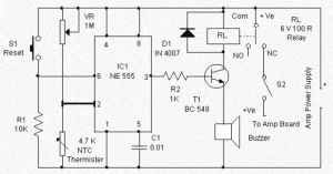
    Now you can protect your HiFi amplifier from damage due to overheating. This circuit will cut off power to the amplifier board at the time the temperature was high. Automatically connect the power when the temperature returns to normal. This circuit uses a sensor NTC Thermister heat and also has a warning sound and reset determination.

    Amplifier circuit protector is using popular timer IC NE 555 as the temperature controlled switch. The trigger pin 2 is connected to a potential divider consisting Thermister VR and NTC. Thus the voltage on pin 2 depending on the resilience and determination Thermister VR. NTC (Negative Temperature Coefficient) Thermister has a high resistance in the normal temperature and the resistance decreases as temperature increases. Threshold pin 6 of IC is used to reset the IC if necessary. When the pin 6 voltage gets higher than the IC pin 2 will reset and the output is low.

    Power Amplifier Protector
    Power Amplifier Protector  Circuits

    Power to the amplifier board is given by (NC) contact is usually connected from the relay and the switch S2. So that power to the amplifier board will be available through the NC contacts of the relay when the relay S2 and the state is not powered. Thermister resistance is governed by VR triggering pin 2 of IC peaks at normal temperatures. When the temperature inside the cabinet amplifier increases, resistance decreases so that it becomes conductive Thermister. This makes the trigger pin 2 of IC is low and its output is high. T1 works so that the relay energizes and the ringing of a bell. This will damage the electrical supply to the amplifier board. Relay will not be automatically powered when the temperature returns to normal.

    Amplifier circuit protectors are very useful to protect your home sound system.
    See More Detail[...]

    Simple 12V fixed voltage power supply circuit diagram

    Here this circuit diagram is for +12V regulated (fixed voltage) DC power supply. These power supply circuit diagram is ideal for an average current requirement of  1Amp. This  circuit is based on IC LM7812. It is a 3-terminal (+ve) voltage regulator IC. It has short circuit  protection , thermal overload protection.  LM7812 IC is from LM78XX series. The LM78XX series IC is  positive voltage regulator IC for different voltage requirements, for example LM7805 IC is made for 5 volt fixed output voltage . There is LM79XX IC series for negative voltage .

    Circuit diagram of 12V fixed voltage power supply

     A transformer(Tx=Primary 230 Volt, Secondary 12 Volt , 1Amp step down transformer) is used to covert 230V to 12V from mains. Here used a bridge rectifier made by four  1N4007 or 1N4003 diode to convert AC to DC . The filtering capacitor 1000uF,25V is used to reduce the ripple and  get a smooth DC voltage. This circuit is very easy to build. For good performance input  voltage should be greater than 12Volt in pin-1 of IC LM7812. Use a heat sink to IC LM7812 for safeguarding it  from overheating.

    See More Detail[...]

    Non Contact Power Monitor

    Here is a simple non-contact AC power monitor for home appliances and laboratory equipment that should remain continuously switched-on. A fuse failure or power breakdown in the equipment going unnoticed may cause irreparable loss. The monitor sounds an alarm on detecting power failure to the equipment. The circuit is built around CMOS IC CD4011 utilising only a few components. NAND gates N1 and N2 of the IC are wired as an oscillator that drives a piezobuzzer directly. Resistors R2 and R3 and capacitor C2 are the oscillator components. The amplifier comprising transistors T1 and T2 disables the oscillator when mains power is available. In the standby mode, the base of T1 picks up 50Hz mains hum during the positive half cycles of AC and T1 conducts.

    Non-Contact Power Monitor Circuit diagram:  
        Non-Contact Power Monitor circuit diagram

    This provides base current to T2 and it also conducts, pulling the collector to ground potential. As the collectors of T1 and T2 are connected to pin 2 of NAND gate N1 of the oscillator, the oscillator gets disabled when the transistors conduct. Capacitor C1 prevents rise of the collector voltage of T2 again during the negative half cycles. When the power fails, the electrical field around the equipment’s wiring ceases and T1 and T2 turn off. Capacitor C1 starts charging via R1 and preset VR and when it gets sufficiently charged, the oscillator is enabled and the piezobuzzer produces a shrill tone. Resistor R1 protects T2 from short circuit if VR is adjusted to zero resistance.

    The circuit can be easily assembled on a perforated/breadboard. Use a small plastic case to enclose the circuit and a telescopic antenna as aerial. A 9V battery can be used to power the circuit. Since the circuit draws only a few microamperes current in the standby mode, the battery will last several months. After assembling the circuit, take the aerial near the mains cable and adjust VR until the alarm stops to indicate the standby mode. The circuit can be placed on the equipment to be monitored close to the mains cable.

    Source : http://www.ecircuitslab.com/2011/06/non-contact-power-monitor-circuit.html
    See More Detail[...]

    Thursday, April 4, 2013

    High power amplifiers

    By organizing the annual CES 2010, Pass Laboratories has recently introduced a new device that is X260.5 mono-block power amplifiers.
    X260.5 offers a power output of 260W and comes with the Super-Symmetry topology features that can improve performance by adjusting the characteristic value of balancing and damping amplifier distortion / interference.


    High-power amplifiers

    X260.5 device brings all the sonic advantages of mono-block operation for A / B high-power amplifiers in a physical package that can be managed device is half the physical size and weight of the device X600.5 Class D mono-block power.

    Simple physical size, weight that can be managed and high strength coupled with great performance make this device as the Pass Laboratories ideal power-amp in any system that refers to a 2-channel and multi-channel format.

    In addition, it also brings flexibility X260.5 combination for consumers who already have a device Pass Laboratories Stereo amp and want to add an additional channel power amplifier that is suitable sonic Laboratories Pass that complements other devices that have been there before.

    As a stand-alone product, X260.5 device is truly amazing. And its existence at this time will quench the thirst of customers with ease. Equilibrium dynamics coupled with tonal accuracy and spectral balance that provides live music by presenting a taste of the extraordinary closeness.

    Pass Labs X260.5 is capable of processing and increase the power transformer and an AC EMI filters, high-speed/soft recovery rectifiers in parallel, the capacitor power supply that is more parallel and supply RC filtering, improvements to the forefront of the input circuit, and the addition of Clas A bias circuit single. This amplifier offers one RCA inputs and one XLR input connectors. And for those who are interested, you can gain amplifier device is worth 11000 USD or about 110 million dollars per pair. Wow, a fantastic price!
    See More Detail[...]